Asia AI ETF KAIT: Investing Across Shifting AI Bottlenecks, from HBM to Photonics to MLCCs and PCBs
AI's Shifting Bottlenecks
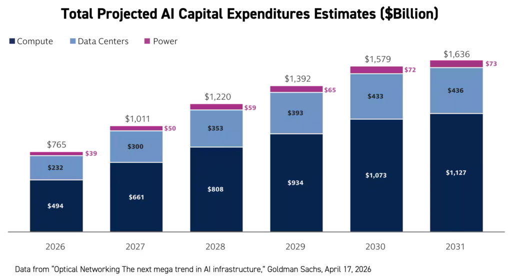
We believe Asia sits at the center of one of the largest physical computing buildouts in history. In May, Goldman Sachs forecasted that baseline global aggregate AI capital expenditures (CapEx) to be $7.6 trillion between 2026 and 2031.1 For perspective, the US interstate system, one of the most expensive projects ever built, cost $704 billion adjusted for inflation.2
We believe Asia is positioned to capture a large part of this investment. Many of the most difficult-to-replicate capabilities within this supply chain are concentrated in Asia. Oxford Economics estimates that Asia accounts for roughly three-quarters of global semiconductor production capacity and the supply of key chipmaking materials.3 In 2025, China, Taiwan, and South Korea together represented 79% of worldwide semiconductor-manufacturing-equipment spending.4 Those figures capture the depth of the region's capabilities, from leading-edge fabrication and memory to precision tools, optical networking, substrates (chip foundations), and thermal management.
Our Asia AI Technology ETF (Ticker: KAIT) is designed to provide targeted exposure to public and private Asian companies building those foundational layers. Rather than concentrating on one processor, model, or application, KAIT seeks to invest across the infrastructure that may benefit as global demand for AI computing expands. We believe today’s AI bottlenecks are dynamic and represented by high-bandwidth memory (HBM), photonics, multilayered ceramic capacitors (MLCCs), and printed circuit boards (PCBs). As production capacity in these sectors increases, new bottlenecks could appear throughout the industry.
AI does not function without infrastructure.
Large language models (LLMs) are trained on vast datasets and then deployed to answer user requests. Both activities require computing clusters: large groups of processors, memory, storage, and networking equipment operating together inside data centers. When any part of that system cannot keep pace, expensive computing resources can sit underused while the facility continues consuming power.
Meeting that demand requires a coordinated supply chain spanning six critical layers:
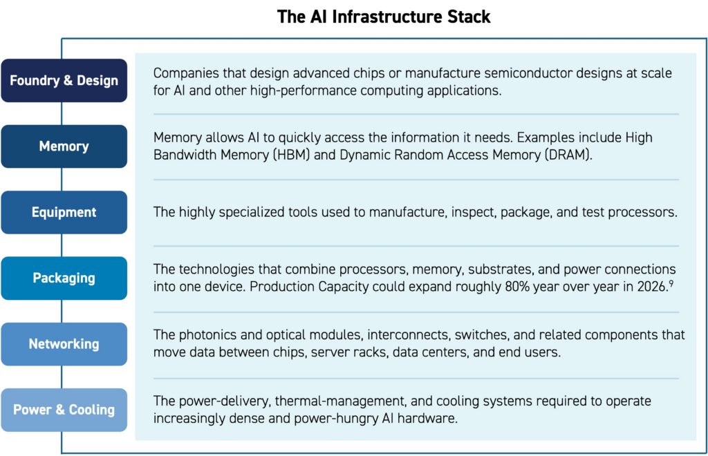
The processor is the brain; HBM feeds it data; packaging puts the components together; networking creates the data highways; power and cooling keep the system running. Better AI models are only valuable if the industry can supply enough chips, memory, equipment, packaging, power, and cooling to support the increased demand.
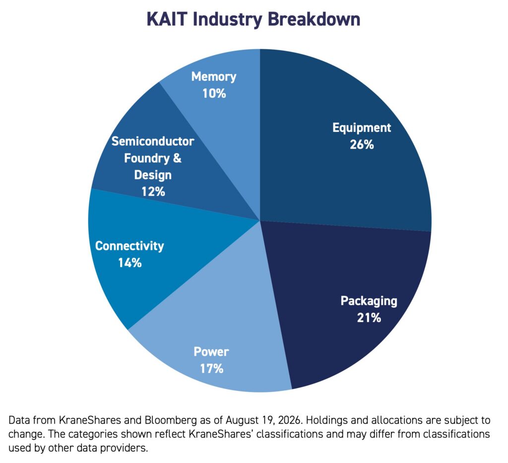
Four ecosystems, four strengths
Taiwan, South Korea, Japan, and China have developed different, complementary strengths. Together, those specialized ecosystems reach nearly every stage of the AI hardware supply chain.
Taiwan: Where advanced chips are manufactured and integrated
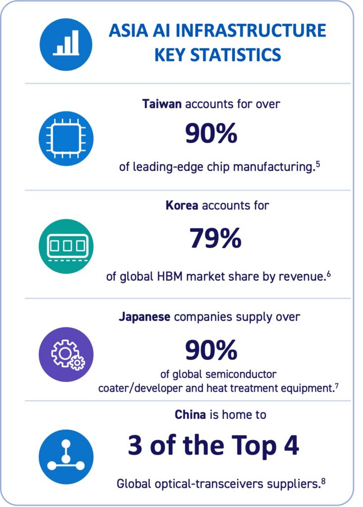
- Taiwan accounts for more than 60% of global foundry revenue and more than 90% of leading-edge chip manufacturing.5
- Within that ecosystem, Taiwan Semiconductor Manufacturing Company (TSMC) held approximately 72% of global foundry revenue in the first quarter of 2026.10
This leadership matters because many of the world's most advanced AI processors are designed elsewhere but depend on foundries such as TSMC to become physical chips.
South Korea: Supplying the memory bandwidth AI requires
- South Korea's defining advantage is memory, particularly HBM.
- In the first quarter of 2026, SK Hynix accounted for 58% of global HBM revenue and Samsung represented another 21%, giving the two Korean companies a combined 79% share.6
- One critical item in this category is multilayered ceramic capacitors (MLCC). These devices filter and stabilize power for processors. AI servers use 10 times as many MLCCs as traditional servers.11
Japan: The Precision Tools and Materials Behind Production
- Japan leads in specialized equipment and materials.
- Japanese companies hold an estimated 60% to 80% of the global market for three critical steps in the chip-making process: single-wafer cleaning tools, batch cleaning equipment, and critical-dimension scanning electron microscopes.7
- Japan’s share of coater/developer and heat-treatment equipment is approximately 90% or more.7
China: Optical connectivity and a broad domestic technology base
- China leads the portfolio in photonics, optical networking, and printed circuit boards (PCBs). Photonics is technology that moves data with light, rather than electricity. PCBs connect each chip component together on one circuit board.
- TrendForce estimates that Chinese optical-module manufacturers will represent approximately 56% of global contract-manufacturing capacity in 2026.12
- Export-oriented suppliers, including fund holdings Innolight, Eoptolink, and Cambridge Industries Group, are expected to account for approximately 46% of worldwide capacity.12
- China is expected to break into further AI infrastructure industries as policy makers push to bolster their advanced manufacturing and design capabilities.
Each country’s strength reflects decades of specialization, capital investment, supplier clustering, engineering expertise, and experience improving manufacturing yields. The result is an ecosystem that is likely difficult, slow, and expensive to replicate elsewhere in the world.
As AI systems grow, the bottleneck can move.
The AI supply chain does not have one permanent constraint. A shortage of leading-edge foundry capacity can be followed by limited HBM supply, advanced-packaging capacity, optical bandwidth, or access to power. As system architectures become more complex, spending may spread to a wider group of enabling companies. KAIT aims to cover each chokepoint.
That shift is visible in semiconductor-equipment data. Global equipment billings reached a record $135.1 billion in 2025. Test-equipment sales rose 55% from the prior year, while assembly and packaging equipment increased 21%, reflecting higher performance requirements for AI devices and HBM.4 Global semiconductor industry association SEMI forecasts total semiconductor-equipment sales of $165.9 billion in 2026 and $229.5 billion in 2028, with growth spanning leading-edge logic, advanced memory, testing, and packaging.13
The cost and complexity of scaling AI may expand the investment opportunity beyond the companies that design processors. Foundries, test systems, memory suppliers, packaging equipment, substrates, networking, power, and cooling are part of the same infrastructure story.
KAIT: Investing across the full AI supply chain.
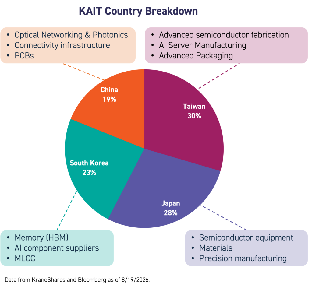
Launched on August 19, 2026, KAIT seeks to provide exposure to Asian companies critical to the global AI supply chain. The portfolio spans Taiwan, South Korea, Japan, and China and includes businesses across compute, memory, equipment, packaging, networking, and power and cooling. It also has the ability to consider select private companies.
U.S.-focused semiconductor strategies emphasize chip designers such as Nvidia, AMD, or Qualcomm. For investors who already own those companies, KAIT is designed to complement that exposure with index guided access to Asian manufacturers addressing critical AI chokepoints and helping to make today's advanced computing systems possible.
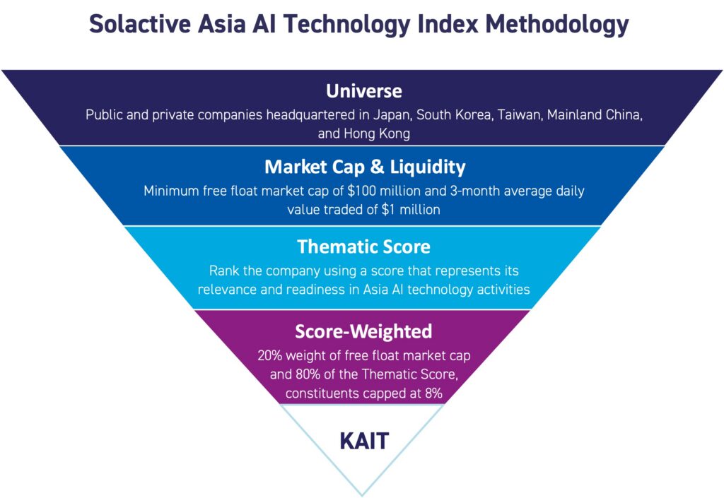
KAIT follows the Solactive Asia AI Technology index. The index methodology is as follows:
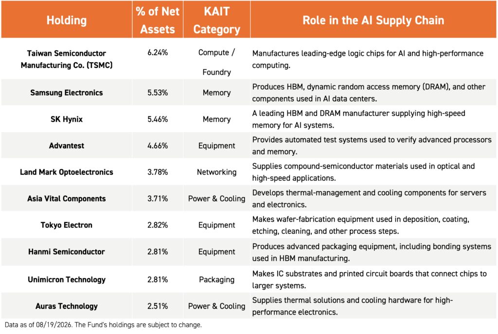
KAIT Top 10 Holdings
Conclusion
We believe AI is increasingly becoming a system-level infrastructure challenge. The fastest processor cannot reach its potential without sufficient memory, advanced packaging, reliable testing, high-bandwidth networking, and efficient power and cooling. Asia's specialized industrial ecosystems occupy critical positions across each of those layers.
The leading AI model may change from one generation to the next. The need to manufacture, connect, power, and cool the underlying infrastructure is likely to remain. KAIT is designed to give investors targeted exposure to the Asian companies building that physical foundation, wherever the next constraint emerges.
Citations:
- Goldman Sachs Global Institute and Goldman Sachs Global Investment Research. “Tracking Trillions: The Assumptions Shaping the Scale of the AI Build-Out.” May 1, 2026.
- Carroll, Todd, and C. Michael Walton. “Opportunities and Challenges for High-Speed Rail Corridors in Texas.” Southwest Region University Transportation Center. September 2011. Conversion: $425B × 333.918 (CPI, July 2026) ÷ 201.6 (CPI, 2006) ≈ $704 billion in July 2026 dollars.
- Oxford Economics. “Asia Chip Export Index May 2026: From Consumer Cycles to Compute Demand.” May 21, 2026.
- SEMI. “Global Semiconductor Equipment Billings Reached $135 Billion in 2025, Up 15% Year-on-Year.” April 7, 2026.
- U.S. International Trade Administration. “Taiwan - Semiconductors Including Chip Design for AI.” December 1, 2025.
- Counterpoint Research. “Global DRAM and HBM Market Share: Quarterly.” June 8, 2026.
- U.S. International Trade Administration. “Japan - Semiconductors.” November 20, 2025.
- LightCounting. “AI Boom Accelerates Transitions Across the Industry Supply Chain.” May 2026.
- Counterpoint Research. “WFE Revenue Up 12% YoY in 2025 Driven by Increased Memory and Advanced-Node Foundry Investments.” April 13, 2026.
- TrendForce. “Strong AI Demand and Early Consumer Electronics Inventory Build Drive Top 10 Foundries to 3.7% QoQ Revenue Growth in 1Q26.” June 12, 2026.
- Samsung Electro-Mechanics. “Samsung Electro-Mechanics Signed KRW 1.0722 Trillion Deal with a Global Major Corporation – AI Server MLCC Supply Contract.” September 1, 2026.
- TrendForce. “China Accounts for 56% of Global Optical Module Manufacturing; Short-Term Supply Chain Decoupling Unlikely Under Potential U.S. Restrictions.” August 5, 2026.
- SEMI. “Global Semiconductor Equipment Sales Forecast to Reach a Record $229 Billion in 2028.” July 14, 2026.
Term Definitions:
Active management: An investment approach in which a portfolio manager selects and adjusts holdings using research and judgment rather than simply tracking an index.
Advanced packaging: Technologies that integrate multiple semiconductor dies, memory, substrates, and connections into a single high-performance package.
AI accelerator: A specialized processor designed to perform compute-intensive AI training and inference more efficiently than a general-purpose processor.
Dynamic random-access memory (DRAM): A common form of working memory that temporarily stores data a processor needs to access quickly.
Foundry: A company that manufactures semiconductor chips designed by other companies.
High-bandwidth memory (HBM): A high-speed form of memory built by stacking multiple DRAM dies (chips) and placing them close to a processor.
Inference: The process of using a trained AI model to generate an answer, prediction, or other output.
IC Substrate: The medium between a semiconductor die and the printed circuit board (PCB)
Optical module or transceiver: A device that converts electrical data into light for transmission and converts received light back into an electrical signal.
Semiconductor equipment: Specialized tools used to manufacture, inspect, assemble, package, and test semiconductor devices.
Substrate: A layered platform that physically supports a chip package and carries electrical signals and power between the chips and a circuit board.
Wafer: A thin foundation for building circuits and microchips.